

ABOUT US
武汉新创元半导体有限公司
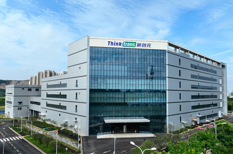
武汉新创元半导体有限公司是2021年通过重组光谷创元和珠海创元,而新成立的企业主体。公司总部位于武汉光谷未来科技城九龙湖街,占地面积约150亩。项目总投资预计60亿元,主要产品是集成电路中的封装基板。公司拥有离子注入镀膜等原创性核心技术,可以制作比常规工艺更精细的线路。公司客户和产品主要针对以下几个领域,存储器、手机、电视主IC等以BT为基材的CSP载板,CPU、GPU、XPU等以ABF为基材的FC-BGA载板,最有特色的是Chiplet对应的大面积、细线宽、高频高速的封装载板。
新创元下属企业骏友电工电子制品(深圳)有限公司,是专门生产柔性线路板(FPC),专注在手机和面板领域。由于使用了离子注入镀膜加成法,特别擅长制作超精细的线路。除了手机和面板的普通FPC外,还能制作毫米波天线、无线充、无硅无磁超净的FPC;应用在手机光学防抖镜头中的VCM线圈、TSA防抖悬浮装置也是公司的特色产品。SMT产线配置完备,可以应对果链的要求。

核心技术
core technology


离子注入气相沉积(IVD)
离子注入气相沉积(Ion Implant Vapor Deposition)技术,新创元独创的全新技术,是通过在基材表面注入金属离子的方式实现基材表面的金属化的一种技术。与传统的化铜实现基材表面金属化不同,该技术是一种基于半导体离子注入的干法技术,新的技术增大了金属与基材的结合力。同时IVD技术对基材更加友好,广泛适用于ABF、BT、PI、陶瓷、LCP、玻璃及常见的线路板用的材料。由于IVD采用干 详细
离子注入加成法(I-SAP)
离子注入加成法(IVD Semi-Additive Process),是基于IVD技术的SAP工艺,并对现有工艺的进一步改善和提升。 区别于传统的半加成工艺,I-SAP工艺具有光滑界面上种子层更薄、图形的补偿更小、线路更均匀、布线密度更高及高频信号传输更友好等优势。 详细

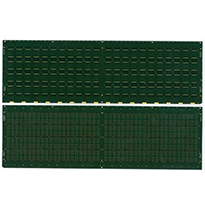
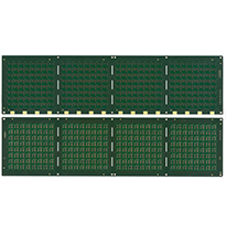
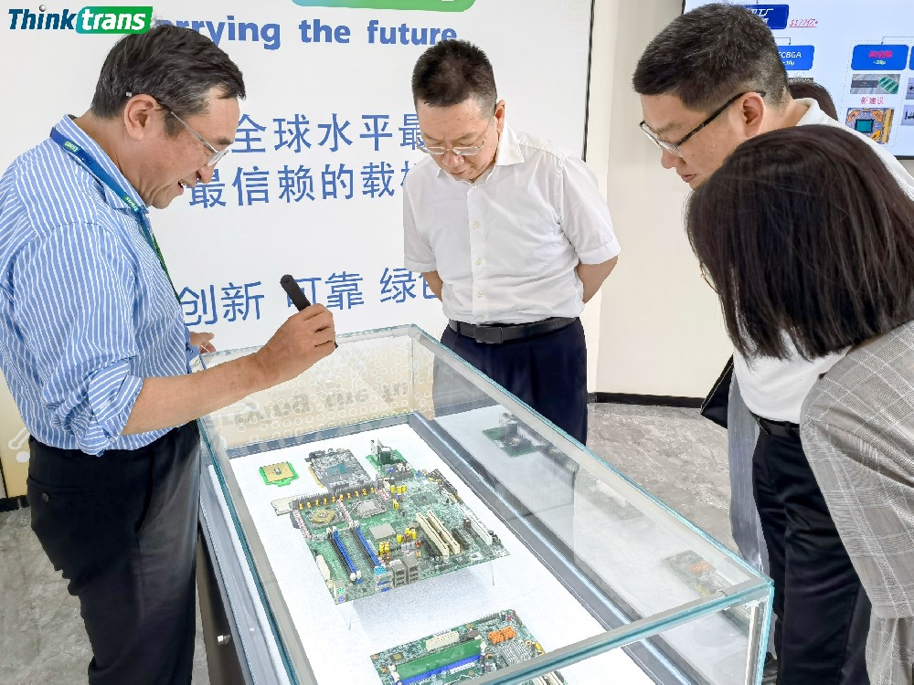
产品展示
Product display


新闻中心
News Center
-
武汉市委组织部领导一行莅临新创元调研
2023-06-22 -
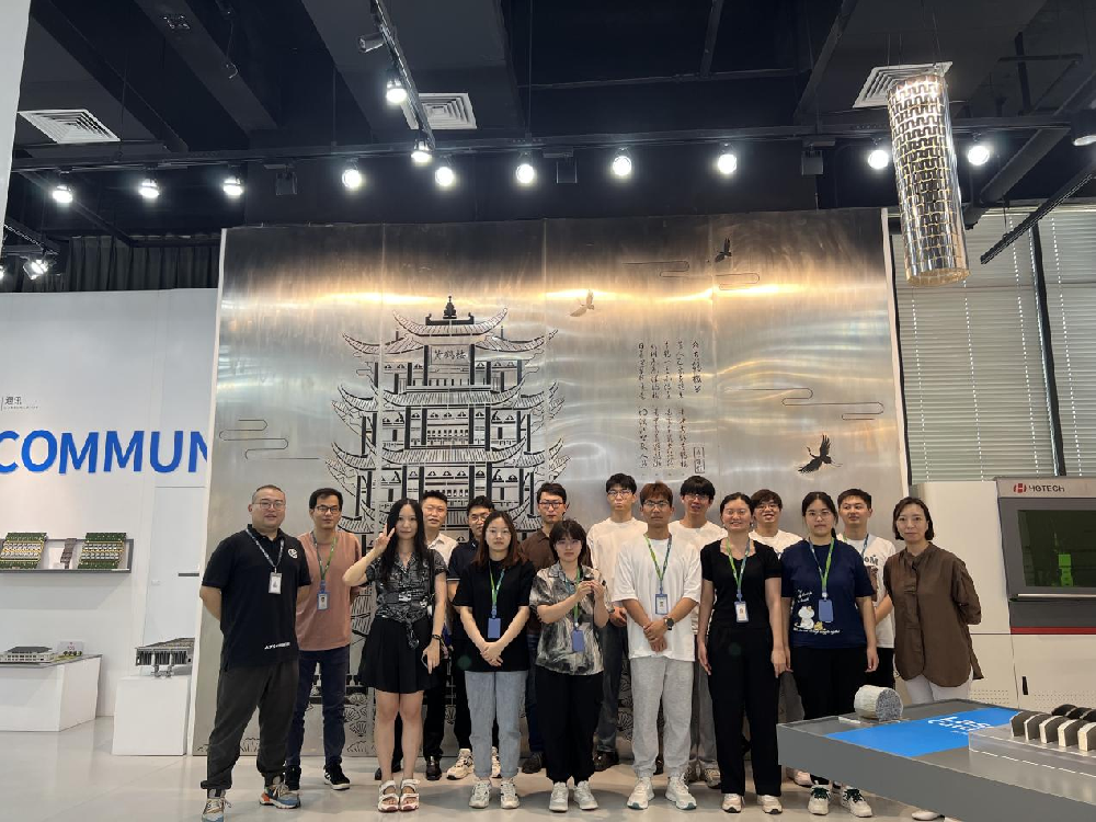
载板事业部青年员工参访华工激光
2023-06-22 -
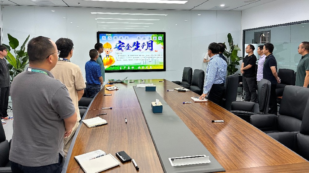
新创元召开安委会全体成员会暨安全生产月活动部署会议
2023-06-15 -
架起“连心桥”、 铺就“成长路”
2023-06-14
